| Sign In | Join Free | My himfr.com |
|
| Sign In | Join Free | My himfr.com |
|
| Ask Lasest Price | |
| Brand Name : | SenYan |
| Model Number : | 2 layers pcb |
| Certification : | ISO14001,ISO13485,ISO9001,IATF16949 |
| Price : | Negotiate |
| Payment Terms : | L/C, D/A, D/P, T/T |
| Supply Ability : | 100000pcs |
| Delivery Time : | 1-30days |
Dear buyer,
Thank you so much for scanning our circuit boards.
As is known, PCB is a customized product, so the unit price is not
real, details please contact me and a quotation will be
offered.Please send us PCB files in Gerber files, ".pcbdoc",
".lay", ".lay6" or ".brd" .
Would like to know more about the product? Send us an inquiry!
Pls feel free to send us Gerber file for latest price!
PCB Bare Board Processing Capacity | ||||
Base Material | Normal Tg FR4, High Tg FR4, PTFE, Rogers, Low Dk/Df etc. | |||
Solder Mask Color | Green, Red, Blue, White, Yellow, Purple, Black | |||
Legend Color | white, yellow, black, red | |||
Surface treatment type | ENIG, Immersion tin, HAF, HAF LF, OSP, flash gold, gold finger,
sterling silver | |||
Max. layer-up(L) | 50 | |||
Max. unit size (mm) | 620*813 (24"*32") | |||
Max. working panel size (mm) | 620*900 (24"x35.4") | |||
Max. board thickness (mm) | 12 | |||
Min. board thickness(mm) | 0.3 | |||
Board thickness tolerance (mm) | T<1.0mm: +/-0.1mm; T≥1.0mm: +/-10% | |||
Registration tolerance (mm) | +/-0.10 | |||
Min. mechanical drilling hole diameter (mm) | 0.15 | |||
Min. laser drilling hole diameter(mm) | 0.075 | |||
Max. aspect(through hole) | 15:1 | |||
Max. aspect(micro-via) | 1.3:1 | |||
Min. hole edge to copper space(mm) | L≤10, 0.15;L=12-22,0.175;L=24-34, 0.2;L=36-44, 0.25;L>44, 0.3 | |||
Min. innerlay clearance(mm) | 0.15 | |||
Min. hole edge to hole edge space(mm) | 0.28 | |||
Min. hole edge to profile line space(mm) | 0.2 | |||
Min. innerlay copper to profile line space (mm) | 0.2 | |||
Registration tolerace between holes (mm) | ±0.05 | |||
Max. finished copper thickness(um) | Outer Layer: 420 (12oz) Inner Layer: 210 (6oz) | |||
Min. trace width (mm) | 0.075 (3mil) | |||
Min. trace space (mm) | 0.075 (3mil) | |||
Solder mask thickness (um) | line corner : >8 (0.3mil) upon copper: >10 (0.4mil) | |||
BGA pad (mm) | ≥0.25 (HAL or HAL Free:0.35) | |||
V-CUT blade position tolerance (mm) | +/-0.10 | |||
Impedence tolerance (%) | +/-5% | |||
Min. legend width (mm) | 0.1 | |||
Fire flame calss | 94v0 | |||
PCBA Processing Capacity | ||||
Processing Service | One Stop PCB Assembly service, include components&plastic mold
sourcing,SMT&DIP assembly and enclosure installation service. | |||
Components Package | Smallest with 01005, various chips package as
QFN,BGA,SSOP,PLCC,LGA.. | |||
Testing | 100% Function Testing before shipment | |||
MOQ | No MOQ(1PCS) | |||
Factory Certificate | ISO9001:2017;ISO13485;ISO16949 | |||


Q1:What are the main products of your PCBA service?
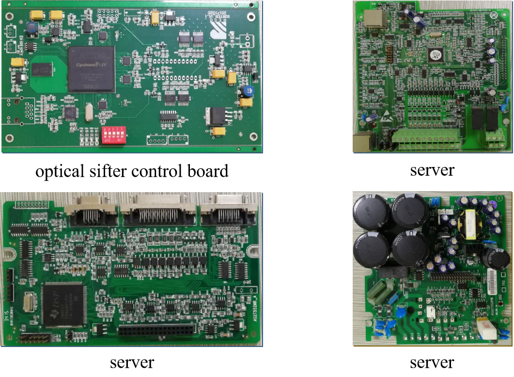
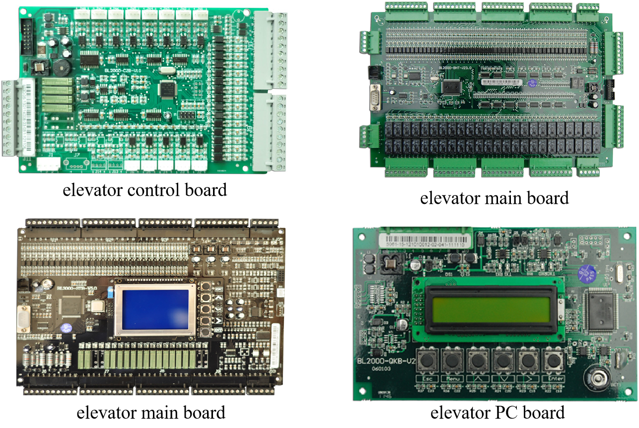
A1:Automotive, medical devices, computer, digital,
telecommunication, elevator, airplane, home appliance etc.
Q2:What is your Minimum Order Quantity (MOQ)?
A2:As for MOQ, we have no request about it. Even 1 Pcs is ok for
us.
Q3:What service do you have?
A3:We can provide OEM ODM EMS service. If your team already have
design files,we can help you do PCB fabrication, PCB/Component
sourcing, PCB assembly,PCBA programming and testing,mold injection,
final product assembly and testing etc.EMS(Electronic Manufacturing
Service),Printed circuit board assembly
Q4: How can we get the PCB/PCBA quotation?
A4: For PCB, pls provide the PCB Gerber files and basic PCB
infos(Material type, board thickness, copper
thickness,soldermask,silkscreen,surface finish etc.)
A4: For PCBA,Pls provide the PCB Gerber files and BOM list.

|


